Molybdenum Disulfide SEM

Introduction
A scanning electron microscope (SEM) is a type of electron microscope that produces images of a sample by scanning it with a focused beam of electrons. The electrons interact with atoms in the sample, producing various signals that contain information about the sample's surface topography and composition. The electron beam is generally scanned in a raster scan pattern, and the beam's position is combined with the detected signal to produce an image. SEM can achieve resolution better than 1 nanometer. Specimens can be observed in high vacuum, in low vacuum, in wet conditions (in environmental SEM), and at a wide range of cryogenic or elevated temperatures.
The most common SEM mode is detection of secondary electrons emitted by atoms excited by the electron beam. The number of secondary electrons that can be detected depends, among other things, on the angle at which beam meets surface of specimen, i.e. on specimen topography.
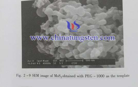
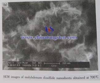
The SEM photography on the left is the image of MoS2 obtained with PEG-100as the template. And the right one is the SEM image of molybdenum disulfide nanosheet obtained at 700℃。
Component
Essential componenets of all SEMs include: eletron gun, electron lense, sample stage, detectors for all signals of interest, display, infrastructure Requirements (power supply, vacuum system, cooling system, vibration-free floor, room free of ambient magnetic and electric fields).
Application
The SEM is widely used to generate high-resolution images of shapes of objects (SEI) and to show spatial variations in chemical compositions: 1) acquiring elemental maps or spot chemical analyses using EDS, 2)discrimination of phases based on mean atomic number (commonly related to relative density) using BSE, and 3) compositional maps based on differences in trace element "activitors" (typically transition metal and Rare Earth elements) using CL.

